FR-4 material PCB fabrication FAQ
Responsibility: We are not taking any responsibility for your Gerber files. We are using them as-they-are for producing the PCBs, so make sure that they comply with all limits and standards.
What kind of file Smart-Prototyping can accept?
Gerber file, Eagle file(.brd) and Altium file(.PCBdoc).
What is the PCB‘s parameter?
Please refer to the PDF.
 PCB parameter.pdf
What can I do if I uploaded the wrong files?
Please send the correct Gerber file to shop@smart-prototyping.com asap, we will use the Gerber file if we didn't start to process the order. But we can not change/cancel your order if the factory already put it on manufacturing line.
Do you have RoHS certification for PCB?
Please refer to the RoHS certification for the PCB material.
RoHS test report.pdfWhat are the rules for controlled impedance traces?
Different trace widths have different impedance, you can download the file to calculate.
What are the rules for PCB panelization?
V-cut/ V-groove
a) Define the v-cut line in outline layer (.GKO/ .GML). e.g. layer 46 in Eagle.
b) The whole board size should be greater than 7cm*7cm, and the sub-board size should be greater than 1.5*1.5cm.
c) You can leave no space between subboards, or you can leave 2-3mm space.
2.03mm spacing panel template.rar
Milling/Slota) Define the milling/slot line in outline layer (.GKO/ .GML). e.g. layer 46 in Eagle.
b) The minimum width for the inner milling is 1.6mm.
Is PCB panelization only for the same PCBs? Can I Panelize by different PCBs?
Yes, you are able to panelize different boards together in one Gerber.
What is the depth of the v-cut?
Normally, the depth of the v-cut this 1/3 thickness of the board.
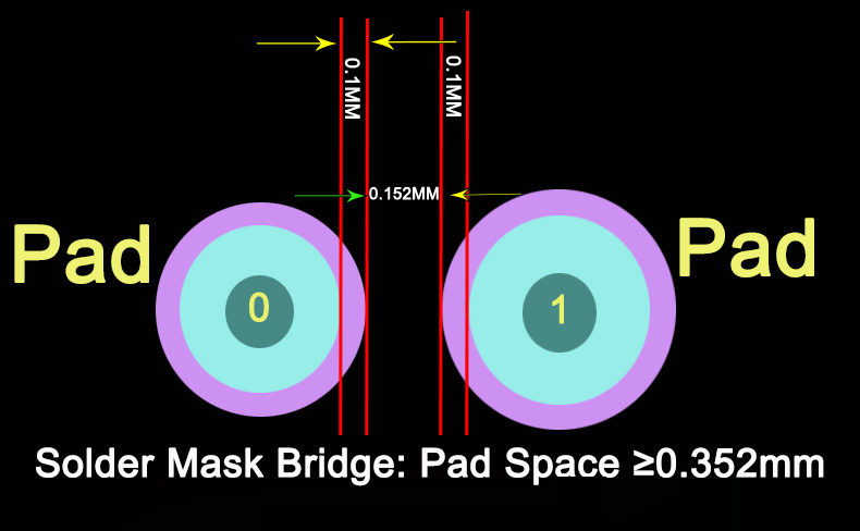
How to define the Solder Mask Bridge?
Pad Space size should be greater than 0.352mm, otherwise there is no solder mask between the pads.
What is the minimum milling slot?
The minimum is 1.6mm for the milling slot.
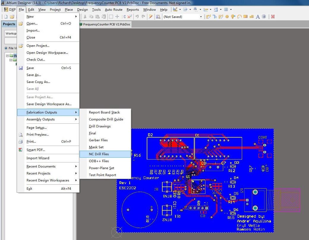
How to export the drill files correctly?
1) Please select EXCELLON instead of Gerber_RS274X when choosing the Device for DrillsHoles, it will help you eliminate the size problem.
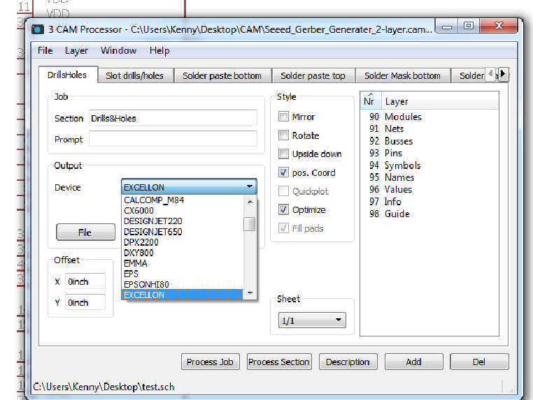
2) If you use Altium, .TXT & .DRL are both acceptable.
What is the range for the drilling hole diameter?
The minimum drill size is 0.3mm and the maximum drill hole size is 6.3mm.
If I do not want any Solder Mask/ drill hole/ silkscreen, what should I do?
Please leave a message "There is no solder mask/ drill hole/ silkscreen" when you check out.
What is the material of solder mask?
The material is photosensitive ink for solder mask.
PCB Production No.
Any boards have the production number, it is used for production record and can be traced if there is quality problem.
But you can assign the position (Top or Bottom). Please add the comment "production number on the Top (bottom) layer" when you check out.
What is the stack-up for 4 layer PCB?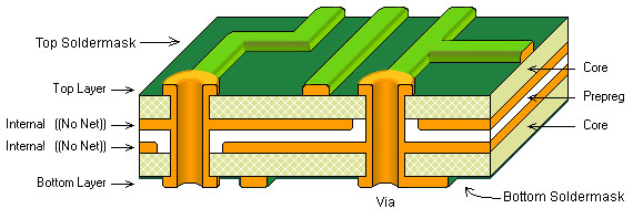
What is the minimum silkscreen text size?
40x6mil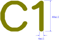
What is the Tolerance of Board Thickness?
± 10%
What is the machining diameter tolerance?
±0.08 mm or ± 3.148 mils
What is the minimum trace width /spacing of 2oz copper thickness?
0.25mm(10mil)
What is the minimum board dimension of V-CUT?
8x8cm
Which layer should I use in EAGLE for milling or slot?
You can use layer 46 (Mechanical layer)and add a note. Thanks!
What is the production time?
The production time is the manufacturing time, it does not include the checking time, packing time and shipping time.
If you need high precision PCB fabrication, please send email to shop@smart-prototyping.com.