FAQ
Shipping and Payment
PCB FAQ
 PCB parameter.pdf
 RoHS test report.pdf
 V-cut/ V-groove
a) Define the v-cut line in outline layer (.GKO/ .GML). e.g. layer 46 in Eagle.
b) The whole board size should be greater than 7cm*7cm, and the sub-board size should be greater than 1.5*1.5cm.
c) You can leave no space between subboards, or you can leave 2-3mm space.
 2.03mm spacing panel template.rar
Milling/Slot
2.03mm spacing panel template.rar
Milling/Slota) Define the milling/slot line in outline layer (.GKO/ .GML). e.g. layer 46 in Eagle.
b) The minimum width for the inner milling is 1.6mm.
You can choose to send us the single board design, we can panelize the board for you.
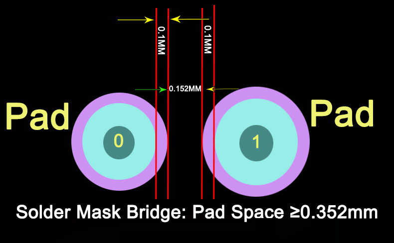
Pad Space size should be greater than 0.352mm, otherwise there is no solder mask between the pads. it happened for most of the fine pitch IC pads, usually there is no solder mask bridge between the fine pitch IC pads, but it will not effect the PCB Assembling process.
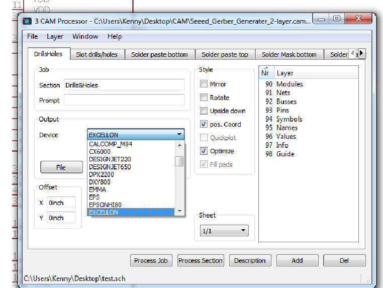
1) Please select EXCELLON instead of Gerber_RS274X when choosing the Device for DrillsHoles, it will help you eliminate the size problem.
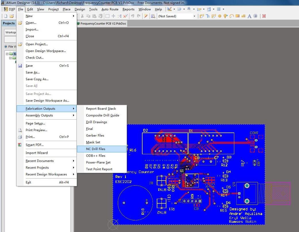
2) If you use Altium, .TXT & .DRL are both acceptable.
Usually solder mask, drill hole, silkscreen is needed for PCB production, without them we need to contact with you to confirm if there is something wrong, but for some Art PCB design, if you don't have one of them, please leave a message "There is no solder mask/ drill hole/ silkscreen" when you check out. So that we don't need to waste your and ours time to confirm again.
But you can assign the position (Top or Bottom). Please add the comment "production number on the Top (bottom) layer" when you check out.
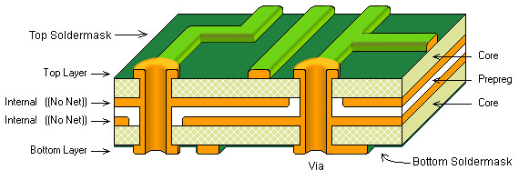
8x8cm.
So if you need to penelize small PCBs, make sure the final big panel's dimension is not smaller than 8x8cm. If there are too many small board in the panel, we will charge you certain additional fee for the V-cut process.
| ITEMS | PRODUCTION CAPABILITY | DESCRIPTION |
Max. Layer | 16 Layers | FR4 accept 1 - 16 layers Aluminium Base PCB: 1 layer Flexible PCB: 1-2 layers Rigid-Flexible PCB: 4 + 2 layers |
| Material Type | 4 types | FR-4, Aluminium Base PCB, Flexible PCB, Rigid-Flexible PCB |
| Max. Dimension | 500 x 500 mm | The online quotation system only accepts up to 500 x 500 mm. If you require a bigger dimension, please contact us |
| Min. Line Width / Space | 4/4 mil | 4/4 mil, 5/5 mil, 6/6 mil (finished copper thickness 1 oz), 10/10 mil (finished copper thickness 2 oz), 15/15 mil (finished copper thickness 3 oz). We strongly suggest increasing the trace width and spacing for 2 and 3 oz. copper thickness |
| Min. Hole Size | 0.2 mm | Minimum mechanical via diameter is 0.25 mm. Minimum laser via diameter is 0.20 mm |
| Hole Tolerance (Mechanical Drilling) | ±0.07 mm | |
| Hole Tolerance (Laser Drilling) | ±0.01 mm | The tolerance of laser drilling hole is ±0.01mm |
| Via Single-side Annular Ring | 3mil | Minimum via is 4 mil. Minimum Components Hole is 6 mil. Increasing via annular ring is good for over current |
| Finished External Copper Thickness | 35 - 105um | The thickness of the board including External plating and finishes |
| Finished Internal Copper Thickness | 17 - 70um | The thickness of the board including internal plating and finishes. Only applies for multiple layers |
| Soldermask Type | Photosensitive ink | White, Black, Blue, Green, Yellow, Red, Purple, Matt Green and Matt Black |
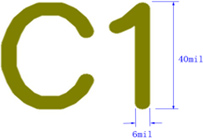
| Min. Silkcreen Letter Width | ≥6 mil | If the minimum silkscreen letter width is less than 0.15 mm, the letters on the boards may not be clear |
| Min. Letter Height | ≥1mm | If the minimum silkscreen letter is less than 1 mm, the letters on the boards may not be clear due to the design |
| Surface Finish | HASL, HASL Lead free, ENIG and OSP | |
| PCB Thickness | 0.1 - 2.4 mm | FR4 material PCB thickness: 0.4/0.6/0.8/1.0/1.2/1.6/2.0/2.4 mm; Aluminium Base PCB thickness: 1.0/1.2/1.6 mm; Flexible PCB thickness: 0.1/0.15 mm |
| Board Thickness Tolerance | ± 10% | |
| Min. Slot Milling Width | 0.5mm to 0.85mm | 0.5mm for Plated Slot, 0.85mm for Non-Plated Slot |
| Space between Routing and Outline | ≥0.25 mm (10mil) | |
| Min. Cutted Hole diameter | 0.6 mm | |
| Panelize by V-cut space | 0 - 0.2 mm space | If you want to separate the panel board by V-cut, keep the space between 0 - 0.2 mm |
| Panelize by Milling space | 1.6 mm | If you want to separate the panel board by Milling, make sure the milling width is over 1.6 mm |
| Impedance control Tolerance | ±10% | |
| Impedance control Bridging | ≥5mil |
First of all, you should check the file carefully before you check out the order, because we will proceed the order as soon as we receive your order. However, if you found the mistake very quickly, and send us an email asap, you will have high chance to avoid the loss.
So, here are the ways you can inform us after you found the mistake (only need to do one of them):
- Send an email to shop@smart-prototyping.com, tell us your order ID.
- Send an online message via online chat at the left-top.
- Send a message via contact us page
Once we receive your message from above channels, we will stop proceeding your PCB order if they are still not on manufacturing line, and replace the file with the correct file you send to us on email.
Please don’t open a charge back case in this case, or cancel the order if you only need to change the file.
The worse case is, it is too late to inform us your PCB file is wrong, as you know, once the PCB is put on fully PCB automatic manufacturing line, there is no way to cancel the order and get refund. So, be careful! That is the most important feature for an electronic engineer!
Yes, you can! We are happy to combine the two orders into one shipment to save shipping cost for you, we will recalculate the total shipping cost, only charge you the difference.
You can choose to place another order separately, pay the shipping cost first, then inform us you want this order ship with another order, we will review your request, then refund the shipping cost difference.
For any other requirements, please contact us via this page https://www.smart-prototyping.com/contact.
The dielectric constant is 4.2 to 4.7 for FR4.
About the trace width of different impedance, please download the tool from this link
If your PCB needs impedance control, please make sure to attach a document of the impedance control trace and target impedance.
We will modify the stack-up and trace width accordingly to meet the impedance requirements.
Yes, we can manufacture special/ irregular shape/outline PCB.
Normally there will be no extra cost for irregular shape, like rectangle shape, round shape, or star shape. However, of the shape is very complex and will increase a lot of milling processing time, we may charge you extra cost.
Here is one of our irregular product: https://www.smart-prototyping.com/Shooting-Star-Learn-To-Solder-Kit
You can download the invoice from the user backend.
1. Go to "View your order history"
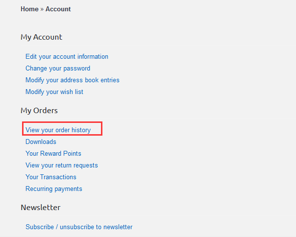
2. Then click the downloading invoice icon.

PCB Assembling
| Assembly Options | SMT (Surface Mount Technology) THT (Through Hole Technology) SMT and THT mixed Single Side Assembly Double Side Assembly Manual Assembly (Without Stencil) Manual with Stencil Assembly Automatic Assembly (Pick and Place machine) |
| Solder Types | Leaded Lead Free (ROHS Compliant) No-Clean Flux is standard |
| Volume | Our minimum order quantity for PCBA is 1. We are capable to handle up to 1 million pcs PCBA. |
| Part Types | Passive Components as small as 0201 package BGA (Ball Grid Arrays) 0.3mm Pitch with X-ray Testing Fine Pitch Components as small as 0.3mm pitch All THT componrnts Accessories like cable, machine parts |
| Component Packaging | We accept parts in Reel, Cut Tape, Tube, Tray, Loose Parts and Bulk. Short-Run Prototype cut tape must be continuous and 12 in. or longer. |
| Board Dimension | Min Board Size (L x W x H): 50mm x 40mm x 0.38mm Max Board Size (L x W x H): 600mm x 400mm x 4.2mm Assembled as single unit or panels (PCBs with sizes smaller than 50mm*40mm will be assembled as panels) |
| Board Shape | Rectangular Round Slots and Cut outs Complex and Irregular (You need panelize the boards in an array and add break-away rails on the longer paralleled edges) |
| PCB Types for Assembly | Rigid PCB Aluminum PCB Flex PCB Rigid-Flex PCBs |
| Lead Time | From 8 hours to 48 hours when PCBs, components and relevant files (PCB files, Centroid file, BOM, PCBA Placement Drawing) are ready. |
| Test Types | MOI (Manual Optical Inspection) AOI (Automated Optical Inspection) X-ray Inspection Short Circuit Testing Power On Testing Functional Testing Design/Build Tester |
| Supported File Formats | ODB++, CAD ASCII, IPC-2581 BOM: .xls, .csv, .xlsx Gerber (RS-274X) Centroid (XY, Pick-n-Place) |
BOM (Bill of Materials) as an Excel, CSV or OpenOffice table with clear defined identifiers for all parts (please download our BOM format)
- Gerber files
- Parts placement drawing
- Centroid data file (This is the machine file which should include X, Y, Theta (Rotation), Side of Board (top or bottom), and Reference Designator. This is sometimes called XYRS data (X,Y, Rotation, Side), pick and place data, or simply XY data. .XLS or .CSV formats are preferred. )
- Other requirements or assembly instructions if applicable

