7 Common and Avoidable Gerber File Mistakes
29/08/2017
7 Common and Avoidable Gerber File Mistakes

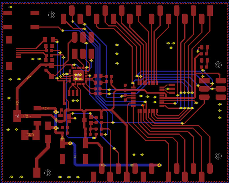
To err is human and like all good errs, making mistakes on Gerber files can be especially frustrating, delaying your timeline and potentially costing you money. So, to spare you (and us!) the frustration of PCB delays and fabrication errors, here’s a list of common Gerber file mishaps we often see and how to avoid them.
Believe it or not, some of the most common mistakes we see in Gerber files is simply forgetting to include a file. To avoid delays, double check your Gerber file includes the following files that are frequently forgotten.
1. Missing drill files
This file is used to determine the size and location of a hole that needs drilled. If you need some holes, we need the files. A .DRL or ile are both acceptable formats to include in your upload.
2. Missing solder mask layers
For two layers or more, the files must include one for top and one for bottom.
If you’ve double checked all the right files are present, make sure to give the remaining mistakes in this list a look through to ensure your Gerber file doesn’t include them.
3. Missing or double outlines
Sometimes we receive files that lack outlines showing where boards should be cut and sometimes we receive files with two boxes around the circuit board. Both situations require us to contact the customer to clarify which outline to follow or where the outline should go.
4. Mismatching PCB size
Sometimes the selected dimension in the placed order and the board dimension in the file does not match. Make sure you have selected the right dimensions for your board in our dropdown menu, to avoid delays.
5. Drill hole placements cut into tracing
Some designs will have a drill hole interrupting the circuitry tracing, but not include a route around the hole.
6. Plated and non-plated holes are not clearly defined
Understand how the CAD software you are using differentiates between PTH and NPTH.
Eagle for example: Non-plated through holes are made by the Hole tool whereas plated through holes are made by the Via tool.
Note: You can create an irregular PTH by drawing a hole in the milling layer over an exposed copper region.
7. Unclear layer labeling
Files for two or more layers will commonly label the top layer “TOP” and the bottom layer “BOTTOM”. However, files with four or more boards will sometimes come with inner layer labels such as “POWER”, “GND”, etc. This causes a delay as clarification is required for layer order.
If you’re creating a four or more layer board, please label the layers to reflect the order with L1, L2 or L2, L3, etc., to avoid confusion.
There are many other less common mistakes that are made on Gerber files everyday, we are all humans after all--even the most practiced Engineer must debug. While solving most of them will ellicit a D'oh, others can take some time to solve. But save yourself some time and irritation and ensure you aren't making the easilly avoidable mistakes listed above.
What's the most vexing mistake you've made on a Gerber?


