PCB Testing: Techniques & Methods
PCB comprises different elements affecting the electronic circuit's overall performance. Tests are carried out to check and optimize the status of these elements using computerized machine software, simple electronic testing equipment and tools, and even basic human inspection. These checks include but are not limited to the following:
Electrical tests, which also include measuring leakage currents
Quality of hole wall
Mechanical resistance test
Quality of the welds
Copper plating was tested with tensile strength, and the following stretching was analyzed.
Cleanliness checks, accounting for weather resistance, humidity, and corrosion
Component alignment, polarity, placement, and orientation
Lamination, which tests the laminate's resistance to peeling by force or application of heat
Environmental tests are particularly necessary for PCBs used in humid environments.
Types of PCB Tests
In-Circuit Testing
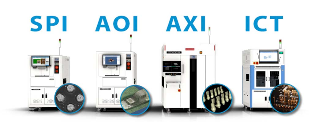
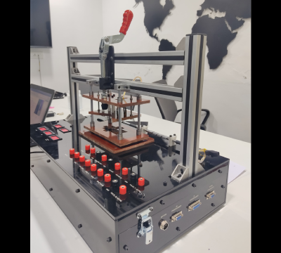
In-circuit testing (ICT) is the most potent type of PCB testing available. It is also known as a "bed-of-nails test," used to verify that each electronic component on the PCB is in its proper location and is operating properly.
Flying Probe Testing
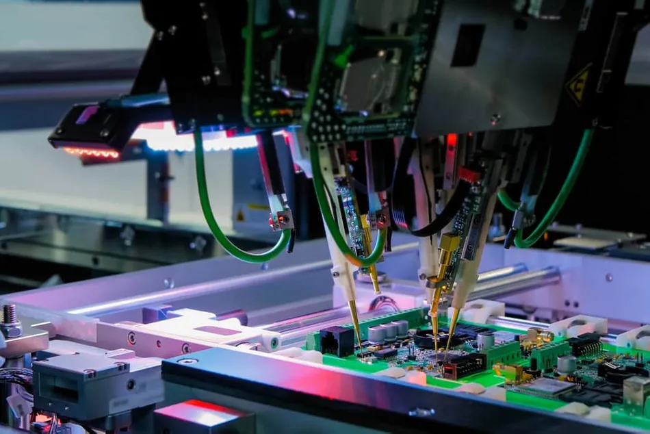
Flying probe test, also known as the fixtureless in-circuit test (FICT), is a type of in-circuit test that operates without specialized test fixtures, lowering the overall cost. With this technique, a basic fixture holds the board in place while a software-controlled program moves test pins about and checks specific test points. Due to its versatility, the flying probe test is well-liked throughout the electronics manufacturing industry.
Automated Optical Inspection (AOl)
AOI is a visual inspection for printed circuit boards that require no contact. Cameras and microscopes are used in AOI to take pictures of the PCB. The software then looks for inconsistencies between these photos and the board's schematic. Technicians may thoroughly inspect each board and spot any issues by this procedure. The board is not powered up during AOI and may not cover all part types.
Burn-In Testing
Burn-in testing is an intensive type designed to analyze PCBs' load capacity and detect early errors. The printed circuit boards go through electrical or thermal testing during this process. In the first instance, electricity is continually applied to the board for about 40 to 160 hours. Another option to examine the PCBs' performance at high temperatures is to expose them to temperatures up to 125 degrees Celsius for 160 hours or longer. The printed circuit boards may frequently also be put through an environmental stress test.
X-Ray Inspection
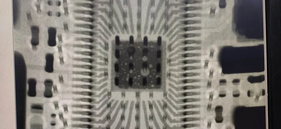
As the name implies, this type of testing is essentially an inspection tool. It is also referred to as AXI. During this test, an X-ray technician can find flaws early in the production process by scrutinizing solder connections, internal traces, and barrels. Inspectingnspect components out of sight using X-ray inspection, like connectors and ball grid array packages with solder joints under the chip. This check typically requires skilled, knowledgeable operators.
Stress Test
Stress Test in PCB testing is a crucial method used to determine the reliability and robustness of a printed circuit board under various conditions. This type of testing evaluates a circuit board's ability to withstand or endure forces or strains that may be placed on it during operation.
Functional Testing
Functional testing, as its name suggests, is aimed at testing a circuit's functionality by simulating the electrical signals capable of stimulating it and observing the results. It is the final stage of PCB inspection and verification. Through the interface connectors, the circuit is accurately powered and electrically stimulated. A software program analyzes the measurements taken at appropriate locations on the PCB and confirms that they match the design requirements.
PCB Testing Equipment
In-Circuit Tester (ICTs)
Camera (AOI)
Automated Test Equipment (ATE)
Test fixtures or jigs
Challenges in PCB Testing
Increasing Complexity: PCB designs are becoming more intricate, with higher component densities and smaller form factors, making it harder to access test points and increasing the risk of undetected defects.
Cost: High-end testing equipment like ATE and X-ray inspection systems can be expensive to purchase and maintain. Testing can also increase production costs, especially if rework is needed due to test failures.
Speed: Setting up and programming ATE systems can be time-consuming, creating bottlenecks in high-volume production environments, particularly with multiple PCB designs.
Accuracy: Despite being designed for precision, testing equipment can still have errors due to calibration issues, software bugs, or human error.
Keeping up with Technology: As new components and technologies emerge, testing procedures and equipment need frequent updates, requiring ongoing investment in equipment and training to stay current.
