


6 Tips to Save You Time on PCB Design
Yahya Tawil, our guest blogger, is an electrical engineer with extensive experience designing PCBs and making, quite frankly, awesome stuff. Here, he'll share 6 tips to keep in mind when designing a PCB.
Every mistake in our design journey contributes to our growth, even if the mistake varies from being a software bug to a PCB design fault. Nevertheless, in most cases, the PCB faults will not only create a headache for you but will also hit the wallet hard after the irreversible process of printing commences.
I can remember the tension, every time a final design is processed for order. The code can be rewritten, and the firmware can be flashed again and again, but a small mistake in PCB design will wreck the whole production slot.
Some of these mistakes can be avoided following some tips and tricks that are not related to an explicit CAD tool. This article assumes that you are at least comfortable with PCB design. These tips may be well-known for experts and mid-level designers, but for beginners, they can save time and headaches.
So, let’s get started.
Tip #1: Reuse footprint/symbols from other libraries
It is very common to see questions on forums and groups asking for the library for a component. Everyone does that at the beginning of the PCB design experience. Designing a library for every component in use is a time-consuming process. Instead, you should reuse the design of another similar component.
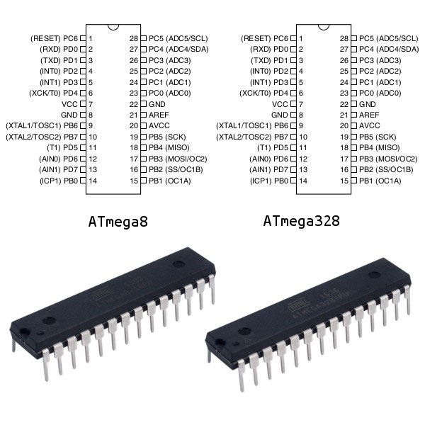
Let’s say you need to use the well-known AVR MCU—Atmega328 and you couldn’t find it in the default ATMEL library in your CAD tool. Only the ATMEGA8 is available. In this case, you can use ATMEGA8 as an alternative to ATMEGA328 as they are identical from PCB perspective; i.e they both have the same package/footprint (dual-in-line 28 pin DIL-28) and the same pinout.
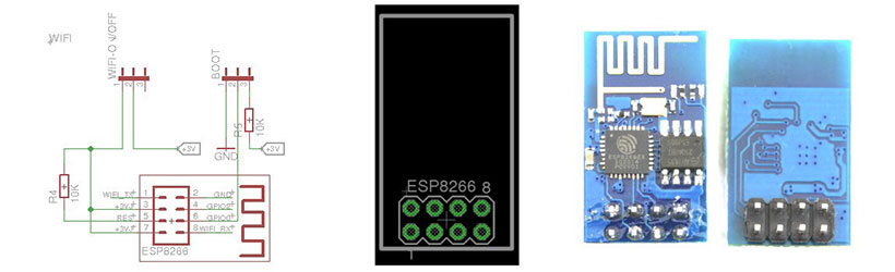
Recently, I wanted to use the WiFi module ESP8266-01, but there was no official library for Espressif products in my CAD tool. Instead of wasting time by creating a new library, I used a 4×2 connector and drew the border of the module around the connector (both in schematic and layout).
Be dynamic enough to reuse other footprints for missing ones when it’s applicable.
Tip #2: Using one PCB design with many different supported footprints
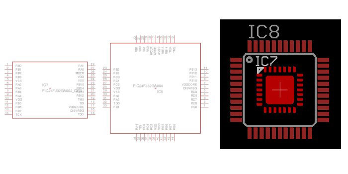
Your product has different versions. All the versions have the same electronic parts, same enclosure, and will use the same MCU family, but with different footprints (many MCU families, like PIC24FJ from Microchip, use different packages to add additional features or peripherals —PIC24FJ128GA006 and PIC24FJ128GA010, for example). In this case, you can either produce a different PCB for each type of design or a single PCB that supports different footprints. The latter option which will cost you less in production.
In the production phase, you can choose to assemble the boards with the desired MCU/parts. The purpose of this trick is not limited to the scenario described above; there are many others out there.
Tip #3: Use the silk layer
The silk layer is a standard for PCB manufacturers and is not just for branding purposes. It's an extremely useful tool for labeling. You can add as many silkscreen layers as you like and when you generate your Gerber file, you can select which ones you want to be printed on the PCB.
If your layout software doesn't already, label your components and add some information about the board. Print the revision number to stay organized, add information about the designer or your company such as your website or brand name, or any other notes you think are important to those using your board.
The Arduino Uno is a good example of silkscreen use. It contains information such as where it was manufactured, it's certifications/RoHS compliance, along with its website and the functions of some components.
Tip #4: Read and follow your manufacture's design rules
Reading the manufacturer's guidelines/capabilities/rules will save you time and the hassle of re-doing designs. For example, you may add VIAs with 0.2 mm drill sizes, while your manufacturer's minimum supported drill size is 0.3 mm. Or you may draw traces with widths less than the minimum trace width supported. You can see our PCB capabilities on the bottom of our PCB order page and among our support pages.
Tip #5: Check parts availability first
Beginner designers who haven’t yet gone through the experience of producing a product, including the supply chain complexity, may use some parts with the assumption that it will be available. Some parts may be obsolete or need a long lead time (the time it takes to receive a part). Don't wait until after sending a finished design to be surprised by the lack of availability.
Changes in this stage are very hard. In some cases, you may need to redesign the whole PCB, especially if the victim part is essential like the MCU, power management IC, etc. I remember when I designed a KIT board with SAM7Sxxx (MCU from ATMEL) with a strict deadline; I used the well-known voltage regulator 7805 (the SMD edition) with the TO-252 package. I told myself that I’ll definitely find it here in the local market in my country, it’s very common. But I was shocked to find only the TO-263 package was available. I didn’t have the time to order the TO-252 from abroad. Sadly, My design failed for a very simple reason: TO-263 can’t fit with TO-252 footprint!
So, always check every single part used in your design before you start designing the PCB.
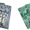
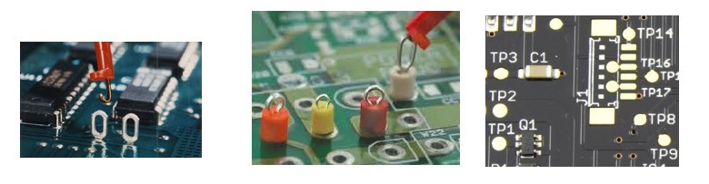
Tip #6: Adding test points
After you print and assemble the PCB, you'll have to edit the firmware, measure voltage or capture some signals using an oscilloscope. You may find some signals hard to reach using the probe, it'll sometimes be impossible. So, add what’s called a test point for each critical signal you think will be tested while developing or maintaining the board.
All images courtesy of original owners
The images above show different types of test points. The first type is suitable for hook-type probes; the loop-shaped test points must be soldered to the PCB. The other type is for normal probes and consists of uncovered (with solder mask) pads.
Have any more tips to add? Leave it below in the comments!
1 Comment(s)

Honestly, I didn't even know what a PCB is until I came across your post. Nevertheless, I appreciate you sharing some tips on how you can save time for your PCB design such as reading and following your manufacturer's design rules. You can never go wrong if you look at the manual to check some of the requirements for designing your PCB. This would definitely serve as a guide or reference for you to be able to determine if your design is indeed plausible or not based on the rules set forth. Thanks.